Scan of electrons and Raman Spectroscopy
The majority of current research is focused on SWNT, that they have better electrical, thermal and mechanical properties than the previously discovered multiparedes (made of concentric tubes). Ten times more resistant than steel and six times lighter, is expected to find many applications in engineering for SWNT composite materials; for example reduce the weight of the spacecraft by at least 50 per cent. Depending on their diameter and chiralidad, the SWNT can show behavior metal or semiconductor, in applications such as threads of nanorreglas and electrical components, while its high electric conductivity (as high as the diamond), make them valid candidates for a sensor range and other applications.
Raman spectroscopy is one of the key analytical techniques to characterize SWNTs. The Raman spectra are used to determine the diameter of the tube, chiralidad, electronic properties and stresses, both in the body of carbon nanotubes or isolated (2-6). In addition, the alignment of carbon nanotubes from carbon in composite materials can be determined by Raman spectroscopy (7). Interest in the Raman of SWNT analysis has increased since the discovery in 2002 that isolated nanotubes show resonant behavior of the Raman, which provides detailed information on the electronic structure (4). This note describes the use of the SCA of Renishaw to the rapid location and isolated SWNTs Raman analysis.
Raman spectroscopy of SWNTs
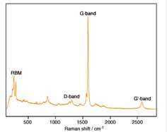
Carbon nanotubes are often as a mass of tangled cords or packages and given the frequency of the MBR (usually in the region 150 cm - 1 to 300 cm - 1) directly depends on the diameter of the tube, the resonant Raman spectrum in this way are used to provide a rapid and simple determination of the distribution of the diameter of the pipe in a sample (2,6,8). The fine-structure seen in the tangential band G depends on the diameter of the tube and chiralidad, and the more intense feature dependent diameter (1590 cm-1) can be used (in conjunction with the RBMs) to help identify individual semiconductor and metallic SWNTs (2). The G band is also affected by the State of oxidation of the carbon nanotubes, (5) and has been used to measure the tension in the SWNTs embedded in a matrix (3). The frequency of the induced disorder D band depends on the diameter and chiralidad of the nanotube, making it heavily dependent on the electronic structure. The G band is the "overtone" second-order of the band D and unlike the D band, its intensity is not reduced in highly ordered crystals. Accordingly, the G band is used to provide electronic structural information in isolated SWNTs (4).
For applications of Raman laboratory, usually provides micromuestreo with a light microscope of degree of research, which allows both simple vision as sending light and collection. The Raman spectra of the "bulk" of SWNTs can be acquired quickly and easily using a Renishaw Raman microscope (see Figure 1 for a typical Raman spectrum acquired with a 785 nm laser excitation). Isolated SWNTs Raman microscopy is more difficult, since the light microscope has insufficient spatial resolution to discriminate discrete nanotubes. Isolated SWNTs Raman analysis has been achieved in the past with a Renishaw Raman microscope scanning through a sample of SWNT of low intensity with the point of laser in steps of 0.5 µm using a table xy controlled up to observe a signal characteristic SWNT Raman microscopeindicating that a SWNT has been located (4). While this technique is successful, the location of nanotubes isolated in this way can be a very time-consuming operation of time.
The structural and chemical Analyzer
The high spatial resolution achieved by techniques SEM (typically 3 to 4 orders of magnitude better than the optical miroscopía) allows the collection of images of unobservable submicron structures with optical microscopy.
Sensitive SEM contrast mechanisms also make it possible to distinguish materials optically identical or similar and in combination with high depth of field, SEM make an ideal technique to see isolated SWNTs.
The majority of SEMs are routinely mounted with team EDS, a technique used for microanalysis x-ray emission. However, EDS is not suitable for samples such as carbon nanotubes that provides only basic information, has poor sensitivity to light elements, and only a small part of the spectrum of x ray is generated from the surface. The success of Raman spectroscopy to the characterization of carbon nanotubes, however, is well documented as described earlier in this article.
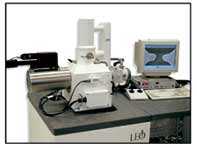
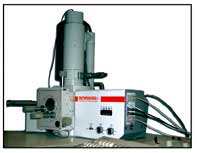
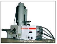
Renishaw structural and chemical Analyzer combines the power of visualization and resolution of SEM with the chemical and physical power of identification of Raman Spectroscopy, allowing users to locate samples with the SEM and characterize their chemical and structural properties with Ramanwithout having to move the sample or optical.
Experimental
The SCA allows the observation of the area of spectroscopic analysis as a point in MicroElectroMechanical rule projected on the surface of the sample in the SEM image. The output of optical fiber from the SCA was connected to a spectrometer Renishaw RM1000 for spectral analysis with excitation 633 nm and 532 nm laser.
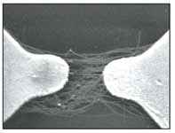
Two samples were analyzed: one shows mass, consisting of a packed mass of carbon nanotubes with a cloudy appearance and a sample of micro scale comprising discrete alienated nanotubes between two separate gold electrodes 1 µm (Figure 4).
Results and discussion
In a first approximation, the frequency of the mode of radial breathing (RBM) in the Raman spectra of carbon nanotubes depends inversely on the diameter of the tubes, 6.8 according to the equation,
wRBM = to / dt where wRBM is the frequency of the MBR in cm-1, dt is the diameter of the nanotube in nm, and a is a constant, depending on the substrate, and has the value of 248 cm-1 nm for Silicon (8). The Spectra indicate tubes of diameter in the range of 0.9 to 1.3 nm nm. The most intense spectra of 633 nm show three maxims in the MBR region, corresponding to the diameter of 1.0 nm (256 cm-1), 1.1 nm (216 cm-1), and 1.3 nm (192 cm-1). Despite indicate diameter of pipe within the same range, the MBR mode in two Spectra 532 nm have various forms, with the spectrum SCA taking a maximum intensity corresponding to a diameter of pipe of 1.0 nm, and the RM spectrum a diameter of 1.3 nm. It is believed to be due to these tubes do not produce an effect of strong at this wavelength enhancement, and because the two spectra are like originate from points of different analysis, because it is difficult to relocate the same point of analysis to transfer samples between instruments.
Mass and microscale samples were tested in House SEM using the SCA with laser excitation 633 nm and 532 nm. Really seems that the specter of microscale nanotubes is much more acute than the sample "bulk". This is the result of the low density of the sample in microscale, by presenting only a few nanotubes resonant structure and well defined in the path of the beam of the laser guidance, producing well-defined discrete vibrational modes.
There are a range of structures and orientations of tubes in the trajectory of the laser beam, making it the bands much wider Raman (not homogeneous broadening) (9) in samples in mass.
The intensities of the Raman signal from the sample of nanotube in microscale SEM Chamber were smaller that the mass, which was expected because there are fewer species to disperse in the trajectory of the beam of the laser. While was observed enhancement of resonance excitation of 532 nm for this show, it was insufficient to reveal RBM. However, because the resonance occurred to a smaller wavelength than in the sample mass, it can be inferred that the sample of nanotube microscale have less diameter than the sample mass (6).
Conclusions
The SEM-SCA adds a new dimension to the analysis of carbon nanotubes, training with the Raman signal nanotubes to be directly observed in the SEM. According to Professor Anna Swan of Boston University, the technology is "really valuable for a reason, one should see if there is more than a pipe in the vicinity that could cause interactions, if there are visible defects or ramificacion tubes, or if there are tops rather than single tubes" (9).
Other applications of nanotechnology, such as autoensamblables structures will also benefit from this technique: too small to be seen by optical microscopy structures can be seen using SEM, and analyzed at the same time using Raman spectroscopy.
Awards
References
- S. Iijima, Nature, 354, 56 (1991).
- A. Jorio, a. g. Souza Filho, g. Dresselhaus, M. S. Dresselhaus, a. k. Swan, M. S. Ünlü, B. B. Goldberg, M. a. Pimenta, j. H. Hafner, C. d. Lieber, Phys. Rev. (B), 65 (15), 155412 (2002).
- C. a. Cooper, r. J.Young, d. Halsall, Composites to: Applied Science and Manufacturing, 32 (3-4), 401, (2001).
- A. g. Souza Filho, a. Jorio, a. k. Swan, M. S. Ünlü, B. B. Goldberg, r. Saito, j. H. Hafner, C. d. Lieber, M. a. Pimenta, g. Dresselhaus, M. S. Dresselhaus, Phys. Rev. (B), 65 (8), 085417 (2002).
- Y. Zhonghoua, l. e. Brus, j. Phys. Chem. A, 104 (47), 10995 (2000).
- M. S. Dresselhaus, p. C. Eklund, Advances in Physics, 49 (6), 705 (2000).
- A. r. Bhattacharyya, T. V. Sreekumar, T. Lui, S. Kumar, l. M. Ericson, r. H. Hauge, r. e. Smalley, Polymer (London), 44 (8), 2373 (2003).
- D. Galkowski, Y.Yumazawa, y. Maniwa, i. Umezi, S. Suzuki, and Ohtsuka, y. Achiba, Synthetic Met, 103, 2555 (1999).
- A. k. Swan, personal communication.

